-
- Executive summary
- Introduction
- Under what conditions would chip exports to China mean fewer chips for the United States?
- BIS needs more information to determine whether exporting existing H200 inventories would result in chip diversion
- New H200 production would divert manufacturing capacity for US customers of more advanced chips
- How many more advanced chips could US customers lose per H200 export?
- Appendix 1: How BIS can assess inventory and capacity diversion risks in export license reviews
- Appendix 2: Estimating maximum H200 and MI325X export volumes permitted under BIS’s January 2026 rule
- Appendix 3: Assessing AI chip input rivalries
- Appendix 4: Detailed US chip loss estimates per H200 export under 100% supply inelasticity of HBM3e
Executive summary
In December 2025, President Trump announced that the United States would permit sales of NVIDIA Hopper H200 chips to the People’s Republic of China (henceforth “China”). In January, the Bureau of Industry and Security (BIS) implemented this decision with a new rule that permits case-by-case export license reviews, allowing the sale of chips up to the performance of NVIDIA’s H200 and AMD’s MI325X.
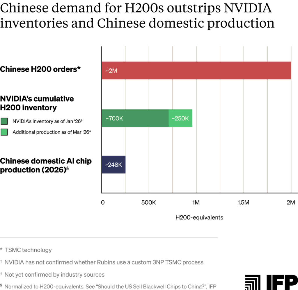
We estimate that this rule could permit exports of up to one million chips.1 Under the terms of the rule, the vast majority of those orders will be for H200s. If fulfilled, this volume would give Chinese AI labs access to about four times more AI chips than China could manufacture domestically this year, normalized for computing power.2
However, under the new rule, license applicants must certify to BIS that exports to China will not reduce chip availability for US-based customers — whether by extending order lead times or by consuming foundry manufacturing capacity that would otherwise go to producing US chips.3 This supply provision reflects ongoing bipartisan Congressional efforts to establish an “America First” AI compute policy, including the proposed AI OVERWATCH Act and the earlier GAIN AI Act.4
The BIS rule does not provide a methodology for evaluating whether a given export to China would divert chips from US customers. This report offers one such methodology. We define a diversion as occurring when:
- Fulfilling Chinese orders reduces chip inventories that US customers would otherwise purchase, delaying US orders; or
- Manufacturing chips for Chinese customers consumes production capacity that would otherwise produce comparable or more advanced chips for US customers.
Based on publicly available information, we judge that:
1. There is weak public evidence that exports of existing H200 inventories at current prices would divert supply from US customers.
Low global sales of Hopper chips since early 2025 point to falling demand for H200 purchases, even as deployed H200s remain in fully utilized. However, customers might be more interested in the H200 at a lower price. China is reportedly being offered these chips at $27,000 per unit, compared to US online market prices of around $30,000–$34,000. Actual pricing varies significantly by customer based on privately negotiated deals: $27,000 could be a markup on what some large US customers would pay, and a discount for others.5
Still, a diversion holds if even one US customer would purchase the chip at the price offered to China. Assessing this requires non-public information BIS should require of license applicants. We provide questions that BIS can ask license applicants and chip suppliers to thoroughly assess diversion in Appendix 1.
2. There is strong evidence that new H200 production would divert manufacturing capacity for US customers of comparable or more advanced AI chips.
Capacity diversion for US customers occurs when: (a) US and Chinese chip orders compete for at least one of the same manufacturing inputs; (b) at least one of those inputs is supply constrained; and (c) inputs allocated to Chinese orders would otherwise have been used to manufacture chips for US customers.
It is highly likely that all three conditions apply to H200 production for China in 2026. First, all leading US AI chips compete with the H200 for the manufacturing capacity of at least one key input: advanced logic wafer production, high-bandwidth memory (HBM), and advanced packaging.
Second, TSMC and major HBM suppliers report that all core production inputs are severely oversubscribed in 2026, such that some customers are offering 100% above regular prices to secure supply.
Third, based on these constraints, the scarce manufacturing resources used to fulfill Chinese orders would almost certainly be otherwise used to produce chips for US-based customers. Roughly 75% of the world’s AI compute is deployed in the United States; ongoing development of the world’s largest AI clusters suggests this trend will continue. This month, NVIDIA reportedly reallocated H200 production capacity to produce new Vera Rubin series chips to meet strong US demand — evidence of the trade-off between H200s and frontier chips. This likely means that the 250,000 H200 chips made for China thus far diverted capacity from the US.6 Meanwhile, US hyperscalers cite a lack of AI compute as a significant constraint on meeting demand for their cloud services, and face worsening order backlogs for Blackwells and Vera Rubins — chips that require the same manufacturing capacity as H200s.7
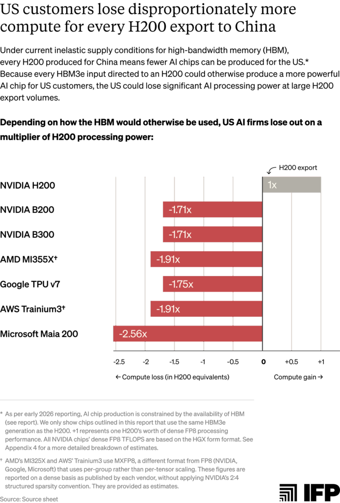
3. In the current conditions of AI chip supply inelasticity, the United States loses more computing power than China gains from every H200 exported.
This is because the same inputs and/or manufacturing capacity are being used to produce less powerful H200 chips than frontier AI chips for US customers. Assuming fully inelastic HBM3e supply, every 100,000 H200s produced for China could delay production of roughly 75,000 Blackwell B200s, which use the same 8-Hi stacks of HBM3e. The resulting compute cost is much steeper: each H200 export forfeits 1.7x the processing performance in lost B200 production.8
Introduction
In recent months, the Trump administration has decided to allow some sales of American AI chips to China. This decision was confirmed with a new rule issued by BIS in January 2026, which permits the case-by-case export of the NVIDIA H200 and the AMD MI325X.9
Released in 2024, the H200 and MI325X sit one architectural generation behind each chip designer’s current frontier.10 Chinese entities have reportedly ordered more than two million H200s as of January — the compute equivalent of approximately one OpenAI-sized AI lab.11 This exceeds NVIDIA’s then-reported inventory of 700,000 chips.
NVIDIA CEO Jensen Huang said in January that the company has “fired up our supply chain and H200s are flowing through the line” to meet demand. This effort yielded approximately 250,000 new H200s as of early March, when NVIDIA reportedly halted further production as it waited for import approvals from Beijing. During this time, it redirected capacity to meet US demand for its next-generation Vera Rubin series. In mid-March, Huang stated that NVIDIA will once again restart H200 production for Chinese customers after it secured regulatory approvals from China.
These Chinese orders add to an already-constrained AI chip supply chain. Last October, NVIDIA reported an expected order backlog of Blackwell and Rubin chips worth $500 billion for 2025 and 2026. In January, Huang told reporters that this backlog has since only “gotten bigger.” This month, he estimated that NVIDIA will sell “at least” $1 trillion of Blackwells and Rubins through 2027, adding “we are going to be short” of customer demand.
Prior to export, US license reviewing agencies must assess whether Chinese orders would divert chip supplies from US customers, and deny exports if they assess this to be the case. How government agencies like BIS evaluate this diversion will determine the quantity and conditions of exports to China.
This report provides one methodology for assessing such diversion. It aims to inform the implementation of “America First” compute policies, including the recently issued BIS rule and proposed legislation such as the AI OVERWATCH Act. We provide our best assessment of whether H200 exports would divert chips for US customers based on publicly available information. Questions that BIS can ask license applicants and chip manufacturers to assess diversion using private information are provided in Appendix 1.
Under what conditions would chip exports to China mean fewer chips for the United States?
American access to advanced AI chips primarily depends on two factors: how many chips designers like NVIDIA have in stock, and how many new chips manufacturers can produce to meet demand. When demand for AI compute outstrips supply, both of these chip sources are finite, making competition effectively “zero-sum” for US and Chinese customers.
Under zero-sum conditions, exports to China would divert chips for American customers if:12
- Fulfilling Chinese orders reduces inventories of a chip that US customers would have purchased, delaying US customer orders. For a diversion of current H200 orders to hold, there must be evidence that at least one US customer would buy the chips for the price on offer to Chinese buyers.13
- Manufacturing new chips for China would consume production capacity that would otherwise produce comparable or more advanced chips for US customers. For capacity diversion conditions to hold, there must be evidence that:
- US and Chinese chip orders compete for at least one of the same manufacturing inputs;
- At least one of those inputs is supply constrained; and
- Inputs allocated to Chinese orders would otherwise have been used to manufacture chips for US customers.
The following sections apply this framework to H200 exports, assessing whether zero-sum conditions hold in 2026. Then, we quantify delayed production of more advanced chips for US customers should H200 orders divert production capacity.
BIS needs more information to determine whether exporting existing H200 inventories would result in chip diversion
BIS’s January rule limits chip exports to half of the aggregate volume shipped to customers for use in the United States. Based on historic sales data, we estimate this could permit exports of between roughly 787,000 and one million H200s.14 As of the time of writing, NVIDIA has a cumulative inventory of approximately 950,000 H200s, assuming no sales of the 700,000 chips reported in late 2025 or the 250,000 additional chips produced thus far in 2026. In theory, it could export most of this inventory and still comply with BIS’s 50% export volume cap.15
However, license applicants must demonstrate to BIS sufficient supplies of the chip in the United States such that a given export would not delay orders for US customers. Whether H200 exports would delay American orders depends on private information, including whether any US customer would purchase H200s at the price offered to Chinese customers.
Limited publicly available information paints a mixed picture:
- Global demand for new H200 purchases has fallen significantly since late 2024.16 NVIDIA has sold few Hopper chips to US or foreign customers (excluding China) in the last year as next-generation Blackwells became available.17 Combined H100 and H200 sales peaked at 791,000 recorded units in Q3 2024, falling to 127,000 units in Q3 2025 and only 23,000 in Q4 2025. NVIDIA’s 700,000-unit H200 inventory in late 2025 (compared to its reported order backlog of 3.6 million Blackwells) further signals weak demand at current prices.18
- But deployed H200s in cloud data centers remain in acute demand. In February, NVIDIA executives said that “even Hopper and much of the six-year-old Ampere-based products are sold out in the cloud,” echoing a late 2025 statement that NVIDIA’s installed Hopper chips were “fully utilized” amid supply constraints. H200 cloud prices broadly reflect this demand: median on-demand cloud rental rates for H200s have risen where other previous-generation chips typically fall — up from approximately $3.20 per H200 GPU-hour at the end of 2024 to approximately $4.00 at the end of 2025.19
- US customers may want H200s at lower prices offered to Chinese customers, especially amid order delays for more advanced chips. Chinese orders have reportedly been placed at around $27,000 per chip, below online market prices of roughly $30,000 to $34,000. At the scale of NVIDIA’s peak roughly 950,000-unit H200 inventory, this price difference amounts to between ~$3 billion and ~$7 billion.20
- However, validating US demand for H200s at prices offered to Chinese customers requires non-public information. Actual chip pricing can vary significantly per customer: large US buyers like hyperscalers often negotiate discounts and may already have the option to purchase H200s below the reported Chinese price — making $27,000 per chip a premium relative to what they would pay.21 For customers purchasing at standard market rates, the same price could represent a meaningful discount. A chip diversion for US customers holds if even one US buyer would purchase the chip at the price offered to China but cannot access it at that price, regardless of whether inventory exceeds permitted export volumes.22
To accurately assess chip diversion, BIS should request that license applicants privately provide current US order and pricing information during license reviews. Appendix 1 provides questions BIS can ask applicants and US customers regarding pricing, order times, and other factors important to determining US chip diversion.
New H200 production would divert manufacturing capacity for US customers of more advanced chips
Future chip production for Chinese customers would divert foundry capacity when shared manufacturing inputs are supply-constrained and would otherwise produce chips for US customers. Based on current severe supply constraints, we judge that additional H200 production would almost certainly divert production capacity for US customers.
Condition 1: Chinese chip orders share manufacturing inputs with more advanced US AI chips
All finished AI chips require three core inputs:
- Advanced logic wafer fabrication capacity, which produces the chip’s main computational die;
- HBM, a specialized memory type stacked vertically to enable high-speed data transfers;23 and
- Advanced packaging, which integrates the logic die and HBM stacks into a finished product.
Semiconductor foundry TSMC dominates global chip fabrication, representing almost 90% of leading-edge chip manufacturing capacity, including AI chips.24 Almost all leading US AI chips (including NVIDIA Hoppers, Blackwells, and Rubins, plus custom chips from AWS and Google) rely on TSMC’s Chip-on-Wafer-on-Substrate (CoWoS) packaging technology.25
Table 1 below summarizes which other AI chip designs are rivalrous with the H200 based on each of these three inputs. We distinguish between “unit” rivalry and “capacity” rivalry for each category:
- Unit rivalry means that two chips compete for the same discrete manufacturing input on a 1:1 basis. When one chip consumes a unit-rivalrous input, that exact input is unavailable to another.26
- Capacity rivalry indicates that two chips share a significant proportion (~70% or more)27 of the same manufacturing equipment or facilities, but do not compete for the exact same discrete input.28 This arises when production of one chip type occupies shared equipment capacity that would otherwise be used or converted to produce a different chip.29
Unit-rivalrous chip inputs would likely be diverted for new H200 production the soonest. Where NVIDIA controls the allocation of unit-rivalrous inputs across its own chip designs (as with HBM3e 8-Hi stacks shared by the H200 and B200), it can independently redirect resources from one chip to another without requiring any change in what TSMC or HBM suppliers produce.30 Based on shared HBM types, the NVIDIA B200 and Google TPU v7 could feel the production trade-offs of Chinese H200 orders most immediately.
The impacts of capacity-rivalrous input diversion for US customers would likely take longer to observe. This is because capacity rivalry requires upstream manufacturers like TSMC and HBM suppliers to adjust their production mix — for instance, producing more HBM3e 8-Hi modules for H200s over 12-Hi modules used by the B200 or Trainium3.31 Because TSMC and HBM suppliers typically plan production allocations well in advance, these adjustments depend on NVIDIA requesting different input quantities and suppliers shifting output accordingly. Capacity-level diversion is therefore more likely to occur under sustained H200 demand than under a short-term production run.32
At a capacity-level, the different HBM generations used by the H200 and Vera Rubin V200 both rely on shared DRAM fabrication at two of the three major HBM suppliers. SK Hynix and Micron, which together represent close to 80% of the global HBM market, use the same process nodes to manufacture DRAM dies for both HBM3e and HBM4.33
H200s also rival more advanced chips on advanced logic wafer fabrication capacity due to TSMC’s shared tooling across process nodes. H200s use TSMC’s custom ‘4N’ 4 nanometer (nm) nodes, Blackwells use TSMC’s enhanced custom 4NP node, and most other chips use 3nm (N3P).34 Despite some key differences in technology, each node shares 85–90% of the same tools according to TSMC, making chips within these nodes subject to many of the same capacity constraints.
Because finished chips all require advanced logic wafer fabrication, HBM, and advanced packaging, a supply constraint on even one introduces zero-sum capacity conditions for rivalrous chips. The availability of these chips is therefore limited by whichever input is scarcest — excess logic wafer fabrication capacity or HBM supply does not yield more chips if there is not enough CoWoS capacity to package them, for example.
We survey current supply conditions for each input below. Technical explanations of unit- and capacity-level rivalry assessments between input types are provided in Appendix 3.
Condition 2: All three shared manufacturing inputs are supply-constrained in 2026
Public reporting and manufacturers’ earnings calls point to severe supply constraints across all three inputs in 2026:
- Requests for TSMC’s most advanced logic wafer fabrication for AI chips exceeds available capacity by 3x. In November 2025, TSMC CEO C.C. Wei said demand for 3nm node wafer fabrication exceeded available capacity by 3x, adding that he had considered wearing a T-shirt reading “no more wafers” to emphasize the shortage. Industry sources indicate TSMC’s 5nm and 3nm production lines will be fully booked with 100% utilization rates through at least the first half of 2026. As a result of this shortage, some customers are reportedly offering double the regular price to secure supply.
- Major suppliers face intense HBM and underlying DRAM shortages. All three major HBM suppliers (SK Hynix, Samsung, and Micron) have confirmed sold-out production capacity through 2026. SK Hynix reported in October 2025 that its HBM, DRAM, and NAND capacity is “essentially sold out” for 2026.35 Micron executives confirmed similar constraints last December, warning that the company can meet only 50-66% of customer demand for memory. Tight DRAM supply (the memory type underlying HBM) is expected to persist beyond this year.36 Due to acute shortages across memory types, NVIDIA has reportedly canceled plans for any new gaming GPU releases in 2026 for the first time in nearly 30 years. It is also expected to cut production of certain gaming GPUs by as much as 30-40% in order to divert memory to AI chips. Meanwhile, American PC companies are looking to Chinese memory suppliers like CXMT for standard DRAM modules.
- TSMC’s advanced packaging capacity is oversubscribed through at least mid-2026. In Q3 2025, TSMC executives said CoWoS capacity is “very tight and remains sold out through 2025 and into 2026.” Due to this shortage, TSMC was reportedly unable to give Google the full packaging capacity it requested (via Broadcom) late last year. NVIDIA has pre-booked approximately 800,000 to 850,000 CoWoS wafers for 2026, representing more than half of TSMC’s projected total output for this year. NVIDIA reportedly confirmed that “CoWoS assembly capacity is oversubscribed through at least mid-2026,” and that additional “ongoing limitations in component supply, such as HBM memory, pose short-term challenges for Blackwell production.”37
Together, these conditions indicate near-total supply inelasticity in 2026. When all capacity is allocated, fulfilling Chinese orders necessarily diverts shared inputs from US customers.
Condition 3: Scarce manufacturing inputs used in H200 production would very likely otherwise serve American customers
There is strong evidence that inputs allocated to Chinese orders would otherwise go to US chip production in 2026:
- There is extreme US customer demand for AI chips rivalrous with the H200. Jensen Huang recently forecast $1 trillion in Blackwell and Rubin sales through 2027 amid what he has called “insane demand” for NVIDIA chips. To meet this demand, NVIDIA reportedly reallocated TSMC capacity from H200s to Vera Rubins in early March — direct evidence that manufacturing inputs used for H200 production would otherwise go to US customer orders. This extends beyond Rubins: In November 2025, Huang told investors that “Blackwell sales are off the charts and cloud GPUs are sold out.” Microsoft executives echoed this in January 2026, stating that “customer demand continues to exceed our supply” for chips used in Azure cloud.38 AWS reported in February that its supply of Trainium3s will be almost entirely committed by mid-2026. Likewise, Google executives said TPU demand outstrips supply to the extent that even its eight-year-old chips remain fully utilized.
- TSMC’s planned 3nm logic wafer fabrication capacity falls short of US demand. SemiAnalysis estimates AI demand will consume roughly 60% of TSMC’s total 3nm wafer output this year, driven mainly by NVIDIA Rubin, Google TPU v7, and AWS Trainium3 production. In 2027, AI is projected to consume 86% of output. This leaves the remainder allocated to non-AI customers like Apple and Qualcomm — two of TSMC’s largest customers that together made up approximately one-third of TSMC’s 2025 revenue. To meet demand, TSMC is expected to expand 3nm capacity to reach between 140,000 and 200,000 wafer starts per month (WSPM) by the end of 2026. Even at the high end, this would fall significantly short of relieving the 3x oversubscription for its 3nm capacity.39 TSMC is also migrating capacity from more mature nodes, including the 5/4nm node used by H200s, Blackwells, and MI325Xs.40 Sustained production of H200s or MI325Xs at the 5/4nm node could therefore delay this migration — resulting in less 3nm production capacity for more advanced US AI chips.
- HBM production bottlenecks will persist due to modest capacity additions. Samsung plans to add nearly 50% HBM production capacity by the end of 2026 with a target of around 250,000 wafers per month. However, this expansion is primarily focused on next-generation HBM4 rather than alleviating the existing shortages of HBM3e used by the majority of chips discussed in this report. Samsung also represents only roughly 20% of the overall HBM market, meaning this 10% capacity addition to the overall market — while significant — is still far below what is required to meet 2026 demand.41 SK Hynix and Micron are building new fabs for HBM production, however neither facilities are expected to reach mass production until at least 2027.
- US demand for AI chips is growing exponentially. The compute required to train frontier AI models has increased approximately 5x per year since 2020. Meanwhile, the inference compute required to run models is expected to account for up to two-thirds of all compute this year. Inference compute is becoming an equally significant source of chip demand as companies deploy AI agents, apply more compute per query, and use AI to accelerate AI R&D.42 In line with this trend, Google has said that its compute capacity must double every six months, resulting in an 1,000x increase over the next 4-5 years. Realizing this compute growth will require substantial quantities of chips.
All three conditions above strongly indicate that producing new H200s for China in 2026 necessarily diverts key manufacturing inputs from US chip production. These conditions likely apply to the roughly 250,000 H200s reportedly manufactured for NVIDIA between early January and early March 2026, when severe supply constraints on advanced logic wafer fabrication, HBM, and CoWoS capacity were already in effect.43 License-reviewing agencies should evaluate exports of these chips — and any additional H200s produced after BIS’s January 2026 rule was issued — for potential diversion of manufacturing capacity for US customers.44
How many more advanced chips could US customers lose per H200 export?
NVIDIA reportedly halted H200 production in early March as it awaited approval from Chinese authorities to import the chips. Just weeks later, Jensen Huang stated that NVIDIA has restarted production.
How NVIDIA ramps up production for Chinese orders determines which US chips and customers are affected. Reallocating existing TSMC capacity to H200s could reduce production of other rivalrous NVIDIA chips like Blackwells and Rubins. If NVIDIA instead secures additional capacity (but TSMC and HBM suppliers remain capacity-constrained overall), H200 production could divert capacity from other US designers — impacting a broader range of chips. We explore these two scenarios below:
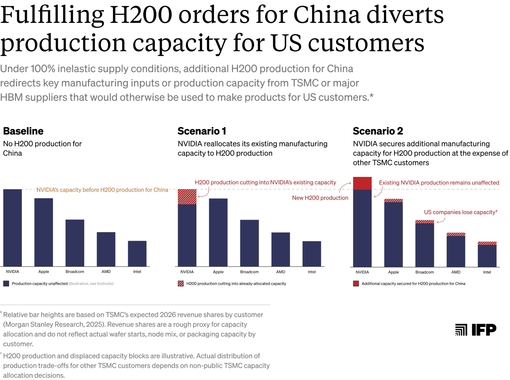
- Scenario 1: NVIDIA manufactures new H200s using its existing TSMC capacity and HBM supply, reducing Blackwell and Rubin production. NVIDIA has secured TSMC manufacturing commitments through at least 2027, including pre-booking more than half of TSMC’s CoWoS capacity for this year.45 Little of this capacity is likely dedicated to H200s by default, given low demand for the chips relative to the more advanced Blackwells and Rubins in the last year. If NVIDIA cannot secure additional TSMC capacity or HBM to manufacture H200s, it would have to redirect existing resources — including wafer starts, HBM modules, and advanced packaging capacity — away from products with rivalrous inputs like Blackwells and Rubins.
- Scenario 2: NVIDIA secures additional TMSC capacity and HBM supply for H200 production, impacting a wider range of US chips. Alternatively, NVIDIA may manage to book additional capacity to manufacture H200s. If TSMC or HBM suppliers are not supply-constrained, further H200 production would have no impact on the supply of other chips. However, assuming that they remain supply-constrained overall, NVIDIA’s booking of additional capacity for H200 production competes for TSMC wafer starts, HBM modules, and packaging capacity that would otherwise be available to other customers. In this case, H200 production for China could impact a much broader set of chips that compete for these same inputs, including Google TPUs, AWS Trainiums, AMD Instincts, and Microsoft Maias.
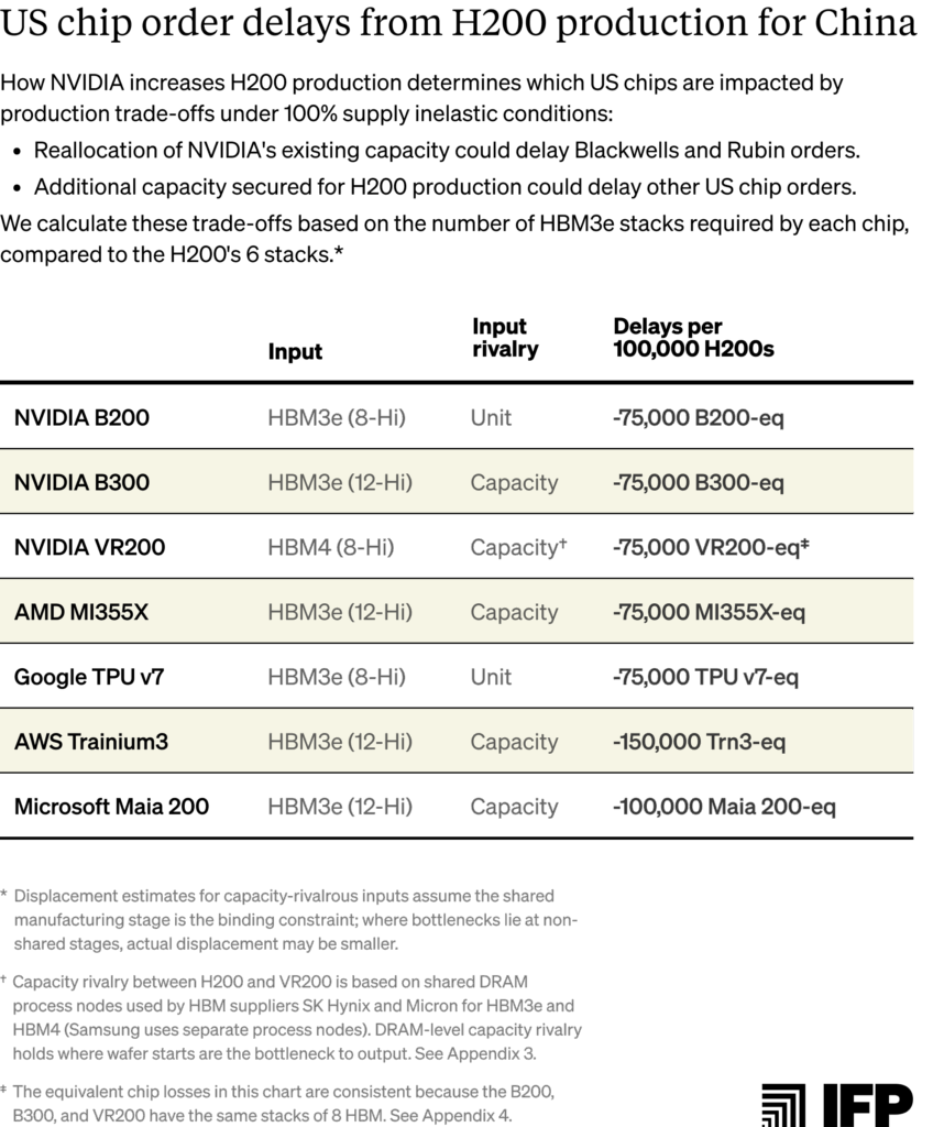
Order delays for US customers due to input or capacity reallocations for H200s are quantifiable based on shared HBM inputs and HBM production capacity. We summarize these delays based on 100% inelastic HBM supply conditions, meaning the figures below represent maximum potential trade-offs.46 Per-chip losses are calculated by dividing the H200’s HBM3e stack count (six) by each rival chip’s stack count.47 A more detailed breakdown of these calculations is provided in Appendix 4.
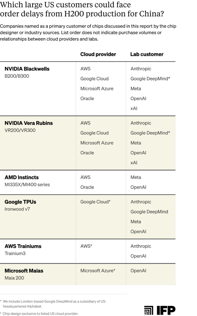
Which US customers would be significantly impacted from H200 production trade-offs?
US cloud providers and frontier AI labs are the largest customers of advanced AI chips. These customers acquire chips in several ways: cloud providers including Microsoft Azure, Google Cloud, AWS, and Oracle purchase chips directly from designers like NVIDIA and AMD. Providers then deploy these chips in data centers that serve external AI labs such as OpenAI and Anthropic, who rent the compute. Other frontier labs like Meta and xAI purchase chips and operate their own infrastructure. Some cloud providers also partner with chip design companies to co-develop custom chips and place orders at TSMC on their behalf — such as Broadcom for Google’s TPUs or Marvell Technology for Microsoft’s Maias and AWS’s Trainiums.48
Every major US cloud provider and frontier AI lab is a customer of NVIDIA Blackwell and Rubin chips. Reallocation of NVIDIA’s existing resources toward H200 production (Scenario 1) could therefore delay orders for all of these customers.49
The customers affected by Scenario 2 (in which NVIDIA secures additional TSMC capacity) depend on which other chip designers lose TSMC capacity as a result. If Broadcom loses capacity, for example, Google may face delays to TPU v7 production, and Google customers including Anthropic, OpenAI, and Meta may face delayed access to TPU compute. If Apple is squeezed, the impact would fall on consumers of iPhones and Macs rather than AI chips.
The actual distribution of production trade-offs ultimately depends on manufacturers’ private capacity allocation decisions and customer contracts. Cloud providers and AI labs using a variety of chips and chip designers face exposure to order delays under both Scenarios 1 and 2, but can more easily absorb delays from any single designer. Alternatively, customers with less diversified chip fleets — such as xAI, which relies almost exclusively on NVIDIA chips — may be more acutely affected by Scenario 1 than by Scenario 2.
The table below highlights major US cloud provider and AI lab customers of each chip discussed in this report:
US customers lose disproportionately more computing power per H200 export than China gains under current zero-sum capacity conditions
Per-chip trade-offs understate the cost to US customers in terms of forgone computing power. More advanced US chips deliver significantly greater processing performance per unit of shared input, meaning that each H200 export costs the United States more computing power than China gains. As the figure below illustrates, each H200 exported to China costs the US nearly 2x the compute in foregone AMD MI355X and AWS Trainium3 production, and close to 2.6x in foregone Microsoft Maia 200 production.50

Appendix 1: How BIS can assess inventory and capacity diversion risks in export license reviews
Publicly available information indicates that exports of NVIDIA H200 (or AMD MI325X) chips would divert chips or manufacturing capacity away from US customers in 2026. BIS must nevertheless make its own determination when reviewing license applications and may request further information from applicants, foundries, and suppliers to accurately assess these risks.51 This appendix outlines the scope of the January 2026 rule’s diversion provisions and proposes questions BIS could use when evaluating compliance.
Scope of the January rule’s supply diversion provisions
BIS’s rule requires that a license applicant “certifies and provides necessary supporting data” demonstrating that:
- “There are sufficient supplies of the product in the United States such that any exports authorized by this license will not be filled if doing so would result in any delay fulfilling any existing or new orders from customers in the United States for end use in the United States for any of its ‘advanced-node integrated circuits’ products (taking into account normal lead times)”; and
- “That global foundry capacity that would otherwise be used to produce similar node or more advanced integrated circuits for end users in the United States will not be diverted to produce commodities authorized by this license for exports to China.”
These provisions apply to more than AI chips. The first covers any of the applicant’s “advanced-node integrated circuits,” while the second covers all “similar or more advanced-node circuits” produced by foundries. Under the Export Administration Regulations (EAR) definition, advanced-node integrated circuits include logic chips produced at 16/14nm or below, as well as certain NAND and DRAM (including HBM). As a result, these provisions cover smartphone chips, gaming GPUs, server CPUs, and other chips beyond AI chips.52
Both provisions protect chip supplies only for customers deploying chips for US end-use — narrower than protecting all purchases by US companies globally. This excludes chips purchased by US companies to install outside the United States, though chips located abroad may still qualify if they support US end-users via remote access.
The questions below assess whether a given export would amount to US order delays due to a supply diversion. Not every question must be answered affirmatively to establish diversion; rather, reviewers should consider the evidence as a whole. An export would more likely result in a diversion if:
- There is unmet US demand at or below the offered export price;
- There are tight supply constraints on shared manufacturing inputs; and
- Evidence suggests that inputs freed by denying the export would serve US customers.
Where applicants cannot provide requested information, BIS should consider whether that uncertainty itself weighs against approval. We flag questions that applicants cannot answer (e.g. regarding upstream production capacity) and that BIS should ask TSMC or other suppliers.
Questions for BIS to assess a diversion of existing chip inventories
1. What is the applicant’s current supply of this product?
- What inventory of this product currently exists in the United States?
- What quantity of the product is currently in production and what are the expected delivery dates?
- Provide a list of current orders, including quantity, price, and expected delivery dates.
- What are the current delivery lead times for this product and for the applicant’s other advanced-node integrated circuit products?
- How do these lead times compare with those over the last 24 months?
2. Is there unmet or pending US customer demand for this product?
- Does the applicant have outstanding or pending orders from US customers for this product?
- What is the expected delivery lead time for the export order under review?
- What price is being offered to Chinese customers for this product, and how does it compare to the prices available to US customers now and over the past six months?
3. Could US demand for this product emerge in the near term?
- What is the applicant’s order backlog for its advanced-node products?
- Has the applicant received formal inquiries or expressions of interest from customers in the past six months?
- Would US customers be willing to purchase the product at the price offered to Chinese customers? If not, what evidence does the applicant have that this is the case?
4. Would fulfilling the export order delay deliveries for US customers?
- Would allocating manufacturing inputs to fulfill the Chinese order extend delivery lead times for US customers?
- If the export were not fulfilled, would those inputs shorten delivery timelines for US customers?
5. Would these chips otherwise be used for end-use in the United States?
For any inquiries, expressions of interest, or orders from US customers:
- Where would the chips be physically deployed if the order were fulfilled?
- What services or workloads would those chips support?
- Would the chips be deployed in cloud or data center infrastructure serving US end-users, even if the infrastructure is located outside the United States?
Questions for BIS to assess a diversion of production capacity
License applicants will not have sufficient visibility into supply or production dynamics outside of their own product lines and thus cannot fully answer all questions provided below. We flag where BIS should ask for more information from upstream manufacturers, such as TSMC or HBM suppliers.
1. Does production of this product rely on manufacturing inputs shared with similar or more advanced chips produced for US customers?
- Does the product rely on the same logic wafer fabrication nodes, HBM supply, or advanced packaging units or capacity used for comparable or more advanced chips sold to US customers?
- BIS can confirm input types with the license applicant (for its own products) and with other US chip designers or trusted market intelligence companies (for other products) where necessary.
2. Are one or more of those shared inputs currently supply-constrained relative to total demand?
- Is global production capacity for these inputs constrained relative to demand?
- BIS can evaluate based on public reporting and private industry conversations (including with US companies and TSMC/HBM suppliers) as necessary.
- Is the applicant’s contracted capacity of that input fully committed?
- For TSMC: “What is the current utilization rate for the fabrication node and CoWoS packaging type used by this product? Is demand for these inputs currently exceeding available capacity, and if so, by how much?”
- For HBM suppliers: “Is production capacity for the relevant HBM type fully committed for the next 12 months? What share of customer demand can you currently fulfill?”
3. Would the manufacturing inputs required to fulfill this export order otherwise be used to produce comparable or more advanced chips for US customers?
- If the inputs required for this export order were not used for the export order, what products would they otherwise be used to produce? Are those products comparable or more advanced chips intended for US customers?
- Provide documentation of existing orders and capacity reservations for those alternative products.
- The applicant cannot answer what TSMC or HBM suppliers would do with freed capacity across their full customer base. For TSMC: “If the wafer starts, CoWoS capacity, or other manufacturing inputs required for this export order were not allocated to it, would there be demand for those same inputs from other US customers?”
4. Would fulfilling this export order extend delivery times for US customers?
- What are the current delivery lead times across the applicant’s comparable and more advanced node products sold to US customers?
- Would allocating manufacturing inputs to fulfill the Chinese order extend the applicant’s delivery lead times for US customers?
- If the export were not fulfilled, would those inputs reduce delivery timelines for US customers of the applicant’s products?
- The applicant cannot assess whether other TSMC or HBM supplier customers’ delivery timelines would be affected. For TSMC/key bottlenecked suppliers: “Would allocating fabrication or packaging capacity to fulfill this export order extend delivery lead times for other customers producing comparable or more advanced chips?”
5. Could fulfillment of this export order delay the migration of fabrication capacity to more advanced nodes used to produce chips for US customers?
- Have foundries communicated plans to migrate the relevant fabrication node used by this product to a more advanced process node that produces chips for US customers within the next 24 months?
- BIS could request additional information from to support this assessment: (e.g., “What is TSMC’s current wafer starts per month (WSPM) capacity at the fabrication node used by this product (e.g., 4N for H200s, N5 for MI325Xs)? What portion of that capacity does TSMC plan to migrate to more advanced nodes (e.g., N3 or N2) over the next 24 months, and on what timeline?)”.
- If so, would sustained production for this export delay that migration?
- This requires information from TSMC: (e.g., “Does demand for NVIDIA’s contracted 4N logic wafer fabrication process for Hopper orders (or AMD’s N5 process for MI325X orders) affect your planned timeline for migrating that node capacity to N3 or N2? If so, by how much?”).
Appendix 2: Estimating maximum H200 and MI325X export volumes permitted under BIS’s January 2026 rule
The rule’s 50% volume condition caps aggregate shipments of a given product to China at half of the volume shipped to US customers for US end-use, measured by total processing power (TPP). Based on historic sales data, we estimate that this could permit NVIDIA to export ~787,500 NVIDIA H200s and ~29,600 AMD MI325Xs, for a combined export limit of between roughly 817,000 and one million chips.
EpochAI estimates NVIDIA made 4.3 million global H100 and H200 sales by the end of 2025. We estimate that roughly half of these sales were H200s, since mass H200 shipments did not occur until around Q3 2024. Assuming that ~75% of H200 shipments were deployed in the United States (consistent with our previous reports and historical trends), the 50% cap permits export of approximately 787,500 H200s. EpochAI estimates AMD sold roughly 79,200 MI325X chips through late 2025. Applying the same assumptions as above yields about 29,600 MI325Xs eligible for export.
Neither company publicly reports sales at this granularity, and US deployment may have exceeded 75% for either chip. To account for the possibility that actual sales were higher than figures captured by EpochAI or that US deployment exceeded 75%, we estimate the combined ceiling for H200 and MI325X exports could reach — but is likely no higher than — approximately one million chips. Given Chinese entities’ high demand for NVIDIA H200s (including orders of roughly two million chips as of early 2026), it is likely that any additional exports between our calculated 817,000 figure and a one million hard limit would be H200s rather than MI325Xs.
The BIS rule uses rolling volume thresholds measured from first commercial US shipment through the license application date. In theory, more US installations permit proportionally more exports to China. In practice, permitted export volumes are unlikely to grow significantly as more performant chips (NVIDIA Blackwells and Rubins and the AMD MI400 series) become commercially available and displace H200/MI325X demand in the US and from ally and partner countries.
Appendix 3: Assessing AI chip input rivalries
This appendix assesses input rivalry between H200/MI325X chips and other advanced AI chips. We define unit rivalry as sharing identical products or processes (1:1 substitutability), and capacity rivalry as competing for the same upstream manufacturing capacity or equipment. Since exact manufacturing processes are proprietary and not publicly disclosed, these assessments represent our best technical judgment based on available industry information.
Advanced logic wafer fabrication
All chips analyzed in this report compete for TSMC advanced logic wafer fabrication capacity, creating capacity-level rivalry. H200s use TSMC’s custom 4nm process (4N), Blackwells use 4NP, MI325Xs use N5, and next-generation chips (Rubins, MI355Xs, TPU v7s, Trainium3s, and Maia 200s) use 3nm.53 While these variants are not unit-rivalrous — meaning they do not share exactly the same processes and technologies — they share 85-90% of the same manufacturing equipment, creating strong capacity-level rivalry.
Within TSMC’s 5nm-family nodes (including N5, N4, N4P, 4N, and 4NP), equipment overlap is particularly high. All variants use the same FinFET (Fin Field-Effect Transistor) architecture and identical core EUV/DUV lithography, etch, and deposition tools. TSMC describes N4 and N4P as “design rules compatible with N5 technology for easy design migration,” indicating that differences between 5nm-family processes are in process parameters — such as specific temperatures and pressures used at each fabrication step — rather than in the underlying equipment.54 Production lines can therefore be reconfigured between these processes by adjusting these parameters without replacing core tools, meaning H200 production consumes TSMC fab capacity that could otherwise be reallocated to Blackwell production under supply constraints.
Capacity rivalry is also significant between 4nm and 3nm nodes. TSMC’s 85-90% shared tooling across advanced nodes allows it to migrate capacity between nodes: it regularly reallocates some portion of its capacity from its more mature nodes to more advanced production, such as from 5nm to 3nm nodes, where demand outstrips supply. Under current constraints, sustained H200 production on 4N could delay planned equipment migration to N3 used for Rubins and other next-generation chips.
HBM
All chips in this report are capacity-rivalrous with H200s, regardless of HBM generation or stack configuration. NVIDIA’s B200, AMD’s MI325X, and Google’s TPU v7 are also unit-level rivalrous with the H200 as all use HBM3e 8-Hi modules.
Though HBM3e 8-Hi and 12-Hi, as well as next-generation HBM4 are not interchangeable as finished products, they compete for many of the same processes at DRAM fabrication,55 TSV formation, and stacking/packaging stages:
- TSV formation: Even when DRAM die production is unconstrained, the common process for creating TSVs can create rivalry between all types of HBM. HBM3e and HBM4 share the same through-silicon via (TSV) equipment. TSVs are formed by etching vertical channels through silicon dies and filling them with copper to create signal and power pathways through the stack. TSV formation uses the same core etching, grinding, and deposition tools across all stack configurations, though the process parameters, such as TSV density and pitch, differ between HBM generations. As the principal process converting standard DRAM wafers into HBM, TSV formation makes all HBM generations and stack configurations dependent on equipment capacity at this stage.
- DRAM die fabrication: HBM3e 8-Hi and 12-Hi use different quantities (8 or 12 layers) of the same HBM3e DRAM dies manufactured on the same process node by each supplier. Notably, SK Hynix and Micron use the same DRAM process nodes (1b and 1β respectively) for both HBM3e and HBM4 production, making H200s capacity-rivalrous with next-generation NVIDIA Rubins and AMD MI400s during DRAM die production bottlenecks (see table below). Capacity rivalry at the level of DRAM fabrication holds for where wafer starts are the binding constraint.
- Stacking and packaging: Stacking and packaging uses the same fundamental techniques for 8-Hi and 12-Hi, with process adjustments for taller stacks. SK Hynix uses mass reflow molded underfill (MR-MUF) bonding for both configurations, applying heat-tolerant material that hardens under heat and pressure. For 12-Hi production, Advanced MR-MUF introduces additional processes — dies are thinned ~40% more to maintain stack heights, and high-heat bursts fuse connective bumps to prevent misalignment. These adjustments run on the same production lines using identical grinding and bonding equipment as 8-Hi production. Samsung and Micron use thermal compression with non-conductive film (TC-NCF) for both 8-Hi and 12-Hi, applying adhesive layer by layer. For 12-Hi, dies are similarly thinned to fit 8-Hi size specifications for later GPU packaging. Again, these are process adjustments within the same TC-NCF workflow and tooling.
Capacity rivalry between H200s and Rubins thus persists at downstream HBM production stages — TSV formation and stacking use some of the same core equipment across HBM3e and HBM4 — though differences in TSV density, stack height, and qualification requirements between different generations mean that downstream capacity is not perfectly fungible. The degree of rivalry therefore depends on which specific production stage is binding. For instance, Hanmi holds a near-monopoly on thermocompression bonding equipment for SK Hynix, meaning SK Hynix’s HBM output is constrained by bonder capacity at least as much as it is by DRAM wafer starts.
CoWoS advanced packaging
All chips in this report are rivalrous with the H200 for TSMC’s CoWoS capacity. AMD’s MI355X and Google’s TPU v7 are unit-level rivalrous with the H200, as all use CoWoS-S packaging.
Almost all advanced AI chips use one of three TSMC CoWoS packaging types: CoWoS-S, CoWoS-L, and CoWoS-R. H200s use CoWoS-S, making it directly rivalrous with other CoWoS-S chips like Google’s TPU v7 at the unit-level extreme supply constraints.
Chips using different CoWoS variants share some manufacturing equipment (including die bonding, dicing, and substrate attachment) but critically diverge on interposer fabrication. CoWoS-S uses a monolithic silicon interposer, while CoWoS-L uses local silicon interconnect (“LSI”) bridges embedded in an organic interposer — each using different materials and fabrication processes. However, TSMC notes that metal types, layer counts, and pitches used to make CoWoS-L’s LSI chips “align with the offering from CoWoS-S,” indicating partial equipment overlap.
This equipment overlap enables capacity reallocation between CoWoS types. In early 2025, NVIDIA CEO Jensen Huang announced plans to migrate CoWoS-S capacity to CoWoS-L for Blackwell chips. Analysts have likewise noted this migration, predicting CoWoS-L would comprise 35% of total CoWoS capacity by Q1 2025 and 45% by Q2 2025.
Appendix 4: Detailed US chip loss estimates per H200 export under 100% supply inelasticity of HBM3e
We provide more granular estimates of US chip losses resulting from H200 exports to China under 100% inelastic HBM3e supply conditions. The table below determines per-chip losses based on the number of HBM3e stacks each chip design requires, detailed in the “HBM3e stack count column.” Per-chip losses are calculated by dividing the H200’s HBM3e stack count (6) by each rival chip’s stack count. For example, each H200 exported displaces 6/8 = 0.75 B200-equivalents under unit rivalry, or 75,000 B200-equivalents per 100,000 H200 exports. Each table represents unit-level and capacity-level rivalry between H200s with the other chip models listed:
-
The BIS rule permits export volumes of a given chip up to 50% of the volume shipped to customers for end-use in the United States to date. Based on historical sales data, we estimate that this could permit NVIDIA to export ~787,500 NVIDIA H200s and ~29,600 AMD MI325Xs, for a combined export limit of between roughly 817,000 and one million chips. See Appendix 2 for the methodology behind these figures. Recorded global sales of NVIDIA H200s are far greater than sales of the AMD MI325X (~two million versus ~79,200 respectively) — meaning that significantly more H200s will be permitted for export under BIS’s rule. As a result, this report focuses on H200 export scenarios. Technical analysis for the MI325X is available upon request.
-
Huawei, NVIDIA’s main competitor in China, produces chips at volumes far lower than Chinese demand. H200 exports give China more total AI computing power than they would otherwise have. For detailed analysis of the potential impacts of this decision, see “Should the US Sell Hopper Chips to China?," IFP.
-
See Appendix 1 for a breakdown of these provisions from the rule text. The rule also includes several other security provisions that are not discussed in this report.
-
The AI OVERWATCH Act is an active legislative proposal in Congress. The GAIN AI Act failed to pass into legislation late last year. See statements from Sen. Elizabeth Warren (D-MA), Rep. Bill Huizenga (R-MI), and Rep. John Moolenaar (R-MI) on the chip diversion provisions of BIS’s January 2026 rule.
-
For example, US hyperscalers making bulk purchases for data centers often receive discounts from standard listed prices. Industry sources indicate that H200s are available to some customers for as low as $17,000-$19,000.
-
The additional 250,000 H200s manufactured in early 2026 and any subsequent production this year should thus be assessed for a diversion of production capacity for US customers, as they were produced when near-total inelastic supply conditions were already in effect (discussed in this report).
-
H200 production for China diverts capacity from Blackwell or Rubin production when NVIDIA reallocates inputs within their limited existing TSMC capacity. If NVIDIA is able to secure additional TSMC capacity for these orders in the future, H200 production would trade off against other chip designs with rivalrous inputs, including Google’s TPU v7 and AMD’s MI355X (assuming TSMC remains overall supply-constrained). We classify “rivalrous inputs” to include unit rivalry, meaning both chip designs use the same input — such as the same HBM3e 8-Hi stack configuration — or capacity rivalry, referring to shared manufacturing inputs to produce different input varieties, such as TSMC’s CoWoS-S versus CoWoS-L advanced packaging.
-
Based on each chip’s dense FP8 processing performance. The B200 delivers approximately 4,500 TFLOPS versus the H200's approximately 1,979 TFLOPS. At 0.75 B200-equivalents foregone per H200 exported, each export costs roughly 0.75 × 4,500 = 3,375 TFLOPS versus 1,979 TFLOPS gained by China, a ratio of approximately 1.7x. These figures are reported on a dense basis by each vendor and are provided as estimates.
-
BIS’s January 2026 rule covers US AI chips up to a technical performance equivalent to the NVIDIA H200 and AMD MI325X, and that are commercially available in the United States as of January 13, 2026. The Trump administration’s separate January 14 decision to apply 25% import tariffs on the H200 and MI325X indicates that these will be the only two chips up for license approvals for the time being. Note that both the January 13 rule and the January 14 tariff decision are executive actions that may later be revised.
-
These are NVIDIA’s Blackwell and AMD’s MI350 series respectively. New product releases this year, NVIDIA’s Vera Rubins and AMD’s MI400 series, will place the H200 and MI325X two generations behind the cutting-edge products available to US customers from these companies by the end of 2026.
-
According to OpenAI and third-party estimates, OpenAI had approximately two million H200-equivalents (measured in TPP) online by the end of 2025.
-
The BIS rule applies to chips shipped for end-use in the United States, and not all purchases by US-headquartered companies writ large. References to "US customers" in this report refer to customers deploying chips for US end-use, which may include chips located abroad that serve US end-users via remote access. An overview of the specific scope of the BIS rule is provided in Appendix 1.
-
If Chinese customers are offered chips at lower prices that US customers would have purchased the chips at, US chip supplies may still be diverted even if the chip is not supply-constrained. The proposed GAIN AI Act from 2025 included a fair pricing provision for this reason.
-
See Appendix 2 for the methodology behind these figures.
-
NVIDIA’s recent decision to continue manufacturing H200s for Chinese customers indicates that it has lower actual inventory than this cumulative 950,000 figure (e.g., NVIDIA has sold chips to non-Chinese customers) or that it intends to keep some inventory in the United States.
-
Demand for AMD’s MI325X has also been low, with EpochAI estimating fewer than 122,000 total sales since the start of 2025. AMD designed the MI325X to compete with NVIDIA’s H200, however delays meant mass shipments only became available in mid-2025, roughly one year after the H200 began shipping. By that time, shipments of NVIDIA’s more powerful Blackwell B200s had already begun, leading many customers to skip over the MI325X entirely. As one illustration, Microsoft reportedly tested the chip but did not place orders.
-
No publicly available information indicates how many MI325Xs AMD has in stock, but given the chip’s relatively poor initial sales performance and AMD’s subsequent pivot to its more advanced MI355X, it is unlikely that AMD has significant inventory of the MI325X.
-
Cloud rental pricing data is measured in dollars per one H200 GPU-hour across 28 cloud providers, captured by GetDeploying. Cloud GPU pricing is an imperfect proxy for demand as rates reflect other factors, including provider margin strategies, competition between providers, and volume pricing. We include it here as directional evidence that H200s retain value, not as a standalone measure of demand.
-
Accounting for NVIDIA’s reported 700,000 H200 inventory as of late 2025 and the additional 250,000 new H200 chips produced as of March 2026, assuming that NVIDIA has sold no chips in this period. 950,000*($30,000-$27,000) = $2.85 billion (low end); 950,000*($34,000-$27,000) = $6.65 billion (high end).
-
For example, industry sources indicate that H200s are available for as low as $17,000 to $19,000. The high variance in H200 pricing makes it all the more important for BIS to ask license applicants about prices available to US and Chinese customers during license reviews (see Appendix 1 for questions).
-
The BIS rule's 50% export cap may leave a buffer between permitted exports and total inventory. For example, if 780,000 chips are eligible for export against an inventory of 950,000, roughly 170,000 chips would remain in the United States regardless of Chinese orders. However, this buffer does not eliminate chip diversion where Chinese customers receive preferential pricing. If chips are offered to China at $27,000 per unit while some US customers face higher prices for the same product, those customers are effectively priced out of inventory that could serve them (even if aggregate chip quantities appear sufficient). BIS should evaluate both whether enough chips exist in the United States, and whether US customers can access them on comparable terms.
-
HBM is manufactured by stacking individual DRAM dies vertically — ‘8-Hi’ and ‘12-Hi’ refer to stacks of 8 and 12 dies respectively, with taller stacks providing greater memory capacity. HBM3e and HBM4 are successive technology generations of these dies, meaning chips can differ on both HBM stack height and generation.
-
We therefore use TSMC’s capacity as a proxy for global foundry capacity in this report.
-
Intel has its own packaging technology known as Embedded Multi-Die Interconnect Bridge (EMIB). September 2025 reports state that NVIDIA will use Intel’s EMIB packaging in the joint development of new PC and data center chips as part of its $5 billion stake in the company. According to more recent reports, NVIDIA is also considering using EMIB packaging for its next-generation Feynman AI chips, which will follow Vera Rubins. Still, mass production of chips using EMIB is not yet reality and thus does not relieve current CoWoS bottlenecks.
-
For example, the NVIDIA H200 and B200 both use HBM3e 8-Hi memory modules, meaning that each module allocated to an H200 results in one fewer module available for a B200.
-
The 70% threshold is a soft boundary. Node migration, where a production line is converted or planned for conversion to a more advanced node, independently establishes capacity rivalry regardless of the precise degree of shared tooling.
-
For example, HBM3e 8-Hi and 12-Hi stacks are not interchangeable as finished units (a chip designed for 8-Hi cannot accept a 12-Hi module), yet both configurations are fabricated from the same same process nodes and nearly identical stacking and packaging tools, meaning they compete for the same manufacturing capacity at the production stage.
-
TSMC typically migrates some portion of its logic wafer fabrication capacity to more advanced process nodes where it has more demand, leveraging the 85-90% common tools between nodes to do so. For example, to expand production at the 3nm node (N3) used to produce NVIDIA Rubins, Google TPU v7s, AMD MI355Xs, and other leading-edge chips, TSMC is reallocating some of this tooling from its 5nm node family (N5), used by H200s (using a custom 4N node) and MI325Xs (using N5) (see Appendix 3). Such capacity rivalry is less direct than unit rivalry in the short term, though it can be significant over time as sustained demand for older-generation production can delay planned migration to more advanced processes.
-
Unit-level rivalry also exists across chip designers at the foundry level: the H200 and Google’s TPU v7 both require CoWoS-S packaging, for example, meaning increased H200 packaging competes directly with TPU v7 production for the same TSMC production lines (assuming that TSMC does not contract packaging to external suppliers). However, this reallocation is TSMC’s decision, not NVIDIA’s. See “Scenario 2” in the following section.
-
Alternatively, sustained H200 production could encourage TSMC to maintain its CoWoS-S advanced packaging output instead of TSMC migrating capacity to CoWoS-L used by more advanced US chips. In early 2025, NVIDIA CEO Jensen Huang announced plans to migrate CoWoS-S capacity (used in H200s) to CoWoS-L (used by Blackwells and Rubins).
-
Large TSMC customers typically reserve TSMC production capacity far in advance to ensure access to scarce manufacturing resources. Customer engagement for advanced node capacity typically occurs 2-3 years ahead of production, with some customers committing pre-payments to lock in capacity. Likewise, major HBM suppliers are currently negotiating volume and pricing with customers roughly 6-12 months in advance.
-
SK Hynix and Micron use the same 1b and 1β process nodes respectively to fabricate DRAM dies for HBM3e and HBM4. Samsung, which represents the remaining approximately 20% of the market, uses a separate 1c process node for HBM4. Global HBM market shares are based on Q2 2025 revenues. See Appendix 3 for further discussion of HBM rivalry across stack heights and generations.
-
TSMC’s standard N4 and N4P processes, as well as its custom 4N and 4NP processes for NVIDIA, sit within the company’s 5nm family, which includes the process used for AMD’s MI325X. NVIDIA has not yet confirmed whether Rubins use a custom 3NP process. Process variants in this family use the same production equipment and share the same facilities. See Appendix 3 for further discussion of shared TSMC tooling for advanced logic wafer fabrication.
-
SK Hynix represented nearly 60% of the global HBM market based on revenue as of Q3 2025.
-
Dynamic Random Access Memory (DRAM) is used in a much wider set of non-AI products including laptops, smartphones, and other PCs.
-
Industry sources state that current H200 assembly and packaging for China is primarily being handled by US-headquartered Amkor, an outsourced semiconductor assembly and test (OSAT) provider with an agreement to use TSMC’s CoWoS technology to package chips. This outsourcing likely reduces the strain of H200 production on TSMC’s internal packaging capacity, though Amkor’s own packaging capacity is unknown.
-
These chips include NVIDIA Blackwells and Maia 200s.
-
Hoppers and Blackwells use custom 4nm (4N/4NP) TSMC nodes, an enhanced version of TSMC’s 5nm (5N) technology. TSMC leadership refers to its 4nm node chips as belonging to its 5N capacity.
-
See the HBM section of Appendix 3 for a breakdown of major HBM suppliers’ market shares and supplies to leading AI chips discussed in this report.
-
See IFP’s Hopper report for further discussion.
-
Reuters reported NVIDIA ramping H200 production on January 6, 2026, though it is likely they directed increased production slightly before this in December 2025.
-
Appendix 1 offers a list of questions BIS could ask license applicants and chip suppliers to assess these and other new H200 chips produced for China.
-
NVIDIA’s October 2025 10-Q filing states that it has manufacturing production, supply, and capacity commitments worth $50.3 billion, “of which substantially all will be paid through fiscal year 2027.” While NVIDIA (and other TSMC customers) may secure key chip supplies months to years in advance, the products that it makes with these supplies are typically determined on much shorter cycles based on demand signals. According to TSMC, customers do not place purchase orders for a particular product far in advance due to rapid advancements in production technologies and chip designs, even when they pre-book capacity. This means that even when capacity is nominally locked in, the products filling that allocation can shift in response to new demand signals, as NVIDIA has recently demonstrated by reallocating capacity from H200s to Vera Rubins in response to delayed export approvals.
-
Actual production trade-offs may differ depending on which TSMC customers are squeezed out of capacity and by how much.
-
For example, each H200 exported displaces 6/8 = 0.75 B200-equivalents under unit rivalry, or 75,000 B200-equivalents per 100,000 H200 exports. More detailed estimates and conversions between US chip losses are provided in Appendix 4.
-
Broadcom and Marvell Technology are US-headquartered fabless semiconductor companies that co-develop custom AI chips for cloud providers and AI labs. Broadcom and Marvell are design partners for Google’s TPUs, Microsoft’s Maias, and AWS’s Trainiums. Both contract TSMC capacity and other manufacturing inputs on their clients’ behalf. Unlike NVIDIA and AMD, which design and sell their own chips, Broadcom and Marvell co-design and procure custom chips for multiple customers simultaneously.
-
This does not necessarily mean that all cloud providers and labs are impacted equally. It depends upon the specific delivery times and contracts negotiated with NVIDIA.
-
Measured by chips’ dense FP8 TFLOP/s. AMD’s MI355X and AWS’s Trainium3 use MXFP8, a different format than FP8 used by other chips in this chart. These are not exact apples-to-apples comparisons and are thus provided as estimates.
-
The rule places all certification and burden of proof on the license applicant, not on upstream suppliers. However, BIS “will routinely confirm the accuracy of relevant elements of the following certifications, using any methods it deems appropriate” — giving it discretion to verify claims directly with foundries, HBM manufacturers, or other suppliers.
-
The EAR defines “advanced-node integrated circuits” using manufacturing technology thresholds rather than chip function. The definition covers: (1) logic integrated circuits produced with a non-planar transistor architecture (e.g., FinFET or gate-all-around) or with a “production” technology node of 16/14 nm or less; (2) NAND flash memory with 128 layers or more; and (3) DRAM with a memory cell area below 0.0026 μm², memory density above 0.20 Gb/mm², or more than 3,000 through-silicon vias (TSVs) per die. Because these criteria are based on fabrication technology and memory density rather than application, the definition encompasses a broad range of advanced chips, not only AI chips.
-
In chip manufacturing, nanometer designations refer to technology generations rather than physical measurements. Smaller numbers indicate denser transistor packing, which improves the chip’s performance and reduces power consumption.
-
This is true for SK Hynix and Micron, representing two of the three major suppliers. Samsung uses a different 1c node process for HBM4.